PCB Layout Design: Steps, Best Practices and Considerations

Introduction
If you’ve ever marvelled at the intricate guts of your favourite gadgets, chances are you’ve encountered the term “PCB layout design.” But what exactly does it entail, and how do you master it? In the blog post, we will demystify the world of PCB layout design, from planning to execution and everything in between.
What Is PCB Layout Design?
Imagine you’re building a house. Before adding the walls and roof, you need a detailed blueprint. The blueprint must outline where each room will be and how they connect. It also shows where the plumbing and electrical wiring will run. In the world of electronics, PCB layout design serves a similar purpose.
A printed circuit board (PCB) is like the foundation of your electronic device. It provides a sturdy platform for all the components to connect and connect. Components such as microchips, resistors, capacitors, and connectors are the building blocks that make your device function.
Think of PCB layout design steps as the architectural process. It involves arranging these components on the board. Like a well-designed floor plan maximises space and functionality in a house, a well-executed PCB layout optimises the performance and reliability of your electronic device.
But it’s not just about slapping components onto a board. Every decision in PCB layout design has consequences. These affect the functionality and performance of the device. Factors like signal integrity, power distribution, thermal management, and electromagnetic interference must be balanced.
In essence, PCB layout design is both an art and a science. It requires creativity to find innovative solutions to design challenges. Technical expertise is also required to ensure that those solutions meet the stringent requirements of modern electronics design.
What Should I Do Before PCB Layout?
Before designing the PCB layout, laying the groundwork is critical to ensure a smooth and successful design process. Here are some key steps to take:
- Begin by defining the requirements and objectives of your project. Understand the purpose of the PCB, its intended functionality, performance specifications, and any specific constraints such as size, cost, and power requirements. This information will serve as the guiding framework for your PCB design.
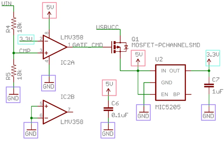
- Develop a comprehensive schematic diagram. A schematic diagram illustrates your circuit’s electrical connections and relationships between components. A well-documented schematic provides a roadmap for your PCB layout. It also helps ensure your design reflects the intended circuit functionality.
- Choose the components you’ll need for your PCB design based on the requirements outlined in your schematic. Consider factors such as component availability, cost, performance specifications, and compatibility with your design goals. Ensure you have datasheets for each component to reference during the layout process.
- Consider the manufacturing constraints and capabilities of your chosen PCB fabrication house. Familiarise yourself with their design rules and guidelines. This includes minimum trace width and spacing, drill sizes, and layer stackup options. Design with manufacturability in mind. It will help avoid costly mistakes and delays during fabrication.
- Consider how your PCB will be assembled and populated with components. Consider components placement, orientation, and accessibility for soldering or automated assembly processes. Designate areas on the board for mounting components, connectors, and any necessary mounting hardware.
- Conduct thorough design reviews with your team or peers. Request feedback and identify potential issues early in the design process. Review the schematic, component selection, and initial layout concepts. Ensure the design aligns with project requirements and design best practices.
- Assemble comprehensive documentation for your PCB design. Include the schematic, bill of materials (BOM), and component datasheets. Add any relevant design notes or specifications. Clear and well-organized documentation will help streamline the design process and collaboration.
Choosing the Right PCB Layout Design Software
There’s no shortage of PCB design software, each with features and quirks. Some popular options include Altium Designer, Eagle PCB, and KiCad. Here are some tips to help you decide.
- Define Your Project Scope: Consider the complexity and scale of your project. A free or open-source tool might suffice for simple projects, while more intricate designs may need a premium solution.
- Learning Curve: Check the learning curve of the software. Opt for tools aligning with your skill level and allowing growth.
- Community Support: A strong user community can be a lifesaver when stuck. Check forums, tutorials, and documentation to gauge each software’s level of community support.
- Cost: Budget constraints are a reality. Balance the features you need with the price of the software. Some tools offer free versions or trial periods, allowing you to test the waters before committing. Remember that product design is expensive due to various electronic product cost factors. So, do not overspend on your tools.
- Future Expansion: Consider the scalability of the circuit design and simulation software. You may start with a basic project, but as you progress, you’ll want a tool to grow with your skills and ambitions.
Basic Steps in the PCB Layout Design Process
Now that you’ve sorted your software let’s talk about the nitty-gritty of PCB layout design. Here’s a brief overview of the basic steps involved:
Component Placement:
- Place high-speed components close together to shorten signal paths and reduce degradation. Group components logically for smooth signal flow.
- Position power-hungry components near power sources to maintain stable power delivery. Keep analog and digital components separate to avoid interference.
- Place heat-generating components strategically and leave space between them to prevent overheating.
Signal Routing:
- Route signals using the shortest paths to minimise degradation and interference. Avoid sharp corners to reduce impedance and signal reflections.
- Maintain consistent trace widths and spacing to ensure signal quality. Use differential pairs for high-speed signals to improve noise immunity.
Ground Plane:
- Include a solid ground plane to reduce electromagnetic interference. Connect all ground pins with short, wide traces to minimise ground loops.
- You must ensure proper isolation and connection points when using split ground planes.
Power Distribution:
- Design a robust network to ensure smooth delivery. Use multiple power planes and low-impedance vias to minimise voltage drops.
- Analyse power requirements for each component and size traces to maintain a stable power supply.
Thermal Management:
- Place thermal vias under heat-generating components to dissipate heat. Use multiple vias for larger components to enhance thermal conductivity.
- Consider adding heating or cooling solutions. A simple device like a fan can maintain optimal temperatures for critical components.
Best Practices in PCB Design
Now that you’ve got the basics down, let’s talk about some best practices to elevate your PCB design game:
Keep it Clean
- Arrange components logically on the PCB to make assembly easier. Group related components together to improve signal flow and reduce clutter.
- Keep trace routing neat and orderly to enhance manufacturability and signal integrity. Minimise crossing traces and maintain consistent trace widths and spacing.
Minimise Noise
- Keep high-speed digital signals separate from sensitive analog components to prevent electromagnetic interference (EMI). Use shielding techniques like ground planes and signal isolation to reduce signal crosstalk and noise.
- Implement proper grounding techniques to minimise ground loops and noise. Options include star grounding and using separate ground planes for different functional blocks.
Test Early, Test Often
- Use SPICE or PCB layout simulation software to analyse your design before prototyping. Conduct signal integrity analysis, thermal simulations, and electromagnetic compatibility (EMC) testing to identify and address potential issues early on.
- Build and test prototypes thoroughly to validate performance under real-world conditions. Use test equipment like oscilloscopes and multimeters to measure signal quality, noise levels, and thermal characteristics.
Stay Flexible
- Include test points throughout your PCB layout for easier debugging and testing.
- Design your PCB with jumper pads, DIP switches, or configurable components. This allows easy modifications and upgrades without major redesigns.
Choose the Right PCB Layout Contractor
Suppose you’re feeling overwhelmed or don’t have the time to tackle PCB layout design alone, fear not! The engineering team at EasyIOT can help you at every step as they provide PCB layout and design services. On top of that, they offer a money-back guarantee, ensuring that you will walk away with a fully functional, manufacturing-ready circuit board.
Contact us to learn more about how we can help you.


