PCB Fabrication in Australia: Understanding How to Make Low-Cost Circuit Boards
Introduction
Hey, DIY enthusiasts and tech wizards! Ready to unlock the secrets behind your favourite gadgets’ brains? Today, we’re delving into the captivating world of PCB fabrication. Have you ever pondered over the magic behind those intricate circuit boards? Get ready for a thrilling ride as we unveil the transparent, concise and downright fun journey of PCB fabrication. We’re here to demystify the process and empower you with valuable insights.
What is PCB Fabrication?
First things first, let’s break it down. PCB stands for Printed Circuit Board. It’s the backbone of nearly every electronic device you own, from smartphones to washing machines. Think of it as a flat, insulating board with a network of copper pathways that connect various electronic components.
PCB fabrication is the process of creating PCBs. It involves multiple steps, including substrate preparation, copper cladding, photoengraving, etching, drilling, plating, solder mask application, silkscreen printing and testing. The manufacturing process brings electronic designs to life, enabling the technology we rely on daily.
Understanding the PCB Fabrication Journey
Let’s talk about how these special circuit boards are made. First, you start with the design phase using PCB design software.
PCB design software is where ideas become circuit board layouts. Designers use different tools in the software to carefully create the paths and connections that make up electronic devices. They focus on sending signals, putting parts in the best spots and managing heat. The software helps them adjust every part of the PCB design.
By applying best practices for PCB layout design, you can ensure that your boards and devices work smoothly while reducing costly mistakes during manufacturing. Every part of the design, from signal strength to heat control, matters greatly for how well the device works and lasts.
Once the PCB design is done, it goes from digital to physical using Gerber files. These files are the standard format for communicating PCB design information to PCB manufacturers. They have all the info needed to make the PCB, like where to put copper, where to drill holes and where to put electronic components. Designers work meticulously to ensure these files follow the rules and standards of the industry.
Once you’ve perfected your design, it’s time to bring your PCB from digital to life through fabrication.
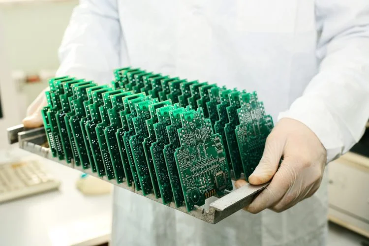
PCB Manufacturing Process
As mentioned earlier, PCB fabrication involves many steps to ensure the final product has good quality. Here is a closer look at each of them:
- Substrate Preparation: The base material, usually a strong fibreglass, is cut to the right size and cleaned well to eliminate dirt.
- Copper Cladding: A thin layer of copper is laminated onto the base material. It covers one or both sides depending on what’s needed for the design. This copper helps electricity move around the PCB.
- Photoengraving: A mask made of photoresist material maps out and covers the desired circuitry pattern on the copper layer. The PCB is then exposed to UV light through a specialised machine, which hardens the copper not covered by the mask.
- Etching: Chemicals wash away the hard and unnecessary copper, leaving only the copper traces that make up the circuits.
- Drilling: Tiny holes, called vias, are drilled into the PCB. These holes help connect different board layers and let through-hole components be put in place.
- Plating: A thin layer of metal, like tin or gold, is put on the copper to make it stronger and easier to solder to. This also helps electricity flow better and stops the copper from rusting.
- Solder Mask Application: A special layer is put over the whole PCB, except where components will be soldered. This layer keeps the copper safe and stops solder from going where it shouldn’t.
- Silkscreen Printing: Finally, important info like component names and logos are printed onto the PCB. This helps people who put the parts together and fix any problems.
- Testing and Inspection: Before they’re sent out, the PCBs are tested a lot to ensure they work correctly. They’re checked for any mistakes or things that don’t look right.
Tips on Optimising Your PCB Design for Affordability
Now that you know how PCBs are made, let’s discuss how to make them cheaper. Here are some tips to help you save money on PCB designs:
- Keep It Simple: Complex designs cost more to make. Try simplifying your design using fewer layers, components and complicated routes. This makes fabrication cheaper and makes your design easier to make reliably.
- Minimise Board Size: Smaller boards need less material and are cheaper. Try to make your PCB as small as possible without losing its function. Smaller designs save on materials and space.
- Use Common Materials: Stick to materials and components that are easy to find. Avoid custom stuff that costs more to make. Choose standard thicknesses, copper amounts and materials to save money.
- Reduce Trace Width and Spacing: Thinner lines and smaller gaps between lines use less material and cost less. But make sure your design still works well and doesn’t overheat.
- Design for Panellisation: Put multiple PCBs on one big panel to save on setup costs. This is good for making a bunch of PCBs at once, especially for small or medium runs.
- Optimise Component Placement: Where you put components can make a big difference in cost. Try to put them where they make the shortest connections and are easy to assemble. Keep things organised and close to where they need to be connected.
- Consider Assembly Techniques: Some assembly methods cost less than others. Surface Mount Technology (SMT) is usually cheaper than Through-Hole Technology (THT) because it’s faster and more automated. But pick what works best for your needs and budget.
- Use Design for Manufacturability (DFM) Guidelines: Use guidelines from your manufacturer to ensure your design is easy to manufacture. This helps catch problems early and makes production smoother and cheaper.
- Work with Your Manufacturer: Talk to your PCB manufacturer to find ways to save money. They can help you pick the right materials and methods to keep costs down and production smooth.
Common PCB Fabrication Mistakes
Even experts mess up sometimes. Here are some common mistakes to avoid:
- Thin Traces: Using too narrow traces can cause problems like weak signals or electrical failures. Consider heat and copper thickness, and ensure your traces can handle the current your circuit needs.
- Wrong Layering: Stacking PCB layers in the wrong order can mess up signals and cost more to fix. Follow industry rules when deciding how to layer your PCB for the best performance and easier PCB manufacturing.
- Ignoring DFM Guidelines: Not following DFM guidelines can make it harder to make your PCB and cost you more money. Pay attention to things like sizes, ring requirements and design rules to avoid problems during production.
- Making Things Too Complicated: Complex designs with extra stuff you don’t need can cost more and make your PCB less reliable. Keep your design simple and focused on what it needs to do instead of adding extra stuff.
- Bad Component Placement: Putting components in the wrong places can mess up signals, cause heat problems and make it harder to assemble them. Put components where they make the shortest connections, reduce signal problems and handle heat well.
- Not Enough Space: Not leaving enough room between traces, pads, and parts can cause shorts or other electrical problems. Ensure your design meets your PCB maker’s minimum space requirements to avoid electrical issues and meet safety rules.
- Skipping Validation: Not checking your design before making it can lead to costly mistakes. Test your design with simulation tools and checks to ensure it works correctly and can be made easily. Fix any problems early to avoid big delays later.
- Ignoring the Environment: Forgetting temperature and humidity can make your PCB unreliable. Design your PCB to handle the conditions it will face, and use materials and processes that can handle tough environments.
Local vs Overseas Fabrication: Pros and Cons
When picking a PCB fabrication partner, you have two choices: local or overseas. Let’s look at the good and bad sides of each:
Local Fabrication:
Pros:
- Faster Turnaround Times: Local PCB manufacturers usually finish jobs quicker than overseas ones. This is handy if you need things done fast or want to test things quickly.
- Easier Communication: It’s simpler to talk with a local PCB manufacturer. You can chat about your needs, fix problems and make changes quickly.
- Better Quality Control: Local PCB manufacturers might do a better job at checking quality. You can watch how things are going and make sure everything’s good.
- Help Local Economy: Picking local helps out your community. It might save on shipping and is better for the environment.
Cons:
- More Expensive: Local services usually cost more because of wages and other costs. This might not be good if you’re on a tight budget or need a lot made.
- Limited Specialisation: Local PCB manufacturers might not be as good at certain things as overseas ones. They might not have the latest tech or special services.
- Capacity Constraint: Local PCB manufacturers might be unable to handle big orders. This could mean longer waits or problems with big projects.
Overseas Fabrication:
Pros:
- Lower Costs: PCB manufacturers overseas often charge less because of lower wages. This is good for projects where you need a lot or want to save money.
- Special Tech: Overseas PCB manufacturers might have better tools and know-how. This means you can do more fancy stuff with your PCB.
- Scalability: Overseas PCB manufacturers can handle big jobs better. They have more space and can make lots of PCBs at once.
Cons:
- Takes Longer: It usually takes longer to get things done overseas because of shipping. This might not work if you’re in a hurry.
- Language and Cultural Barriers: Sometimes, it’s hard to understand each other because of language and culture differences. This can cause delays or mistakes.
- Quality Control Issues: It’s harder to keep an eye on quality when you’re far away. This might mean you get PCBs that aren’t as good as you hoped.
Ultimately, picking local or overseas depends on what you need, how much you can spend and how much control you want. Thinking about the good and bad points can help you decide what’s best for you.
Choosing the Right PCB Fabricator
When selecting the perfect PCB fabricator for your project, you want to ensure you make the best choice. Crucial factors to consider include quality, cost lead time and communication.
If you’re in Australia, don’t miss out on EasyIOT, a contract electronics design and PCB manufacturing company. With headquarters in Sydney and manufacturing facilities in China, we can be your ideal partner for PCB fabrication in Australia. We offer competitive pricing without compromising quality. Our typical turnaround time of 2-4 weeks ensures prompt delivery, and with no minimum order quantity (MOQ), we accommodate projects of all sizes.
And there you have it, folks! A transparent, concise, and fun guide to PCB fabrication. Whether you’re a seasoned engineer or a hobbyist tinkering in your garage, understanding the PCB fabrication process is essential for bringing your electronic creations to life. So, design that next big thing and let the PCB fabrication journey begin!