What to Expect from a Prototype PCB Assembly Process
The trip to create a resilient and reliable prototype PCB assembly starts well before placing the first components on a board. A printed circuit board (PCB) prototype serves as a preliminary version of your circuit board that helps test and assess designs before manufacturing.
Your prototype PCB plays a crucial role beyond the manufacturing process as it represents the core of state-of-the-art design refinement and confirmation. The prototype circuit board transforms through different shapes to become a functional electronic product. Professional PCB prototyping services can provide test boards with up to eight layers that meet quality standard IPC1 specifications using standard RF-4 material. Small-scale testing typically requires 5 to 100 pieces with a build time of four to five business days.
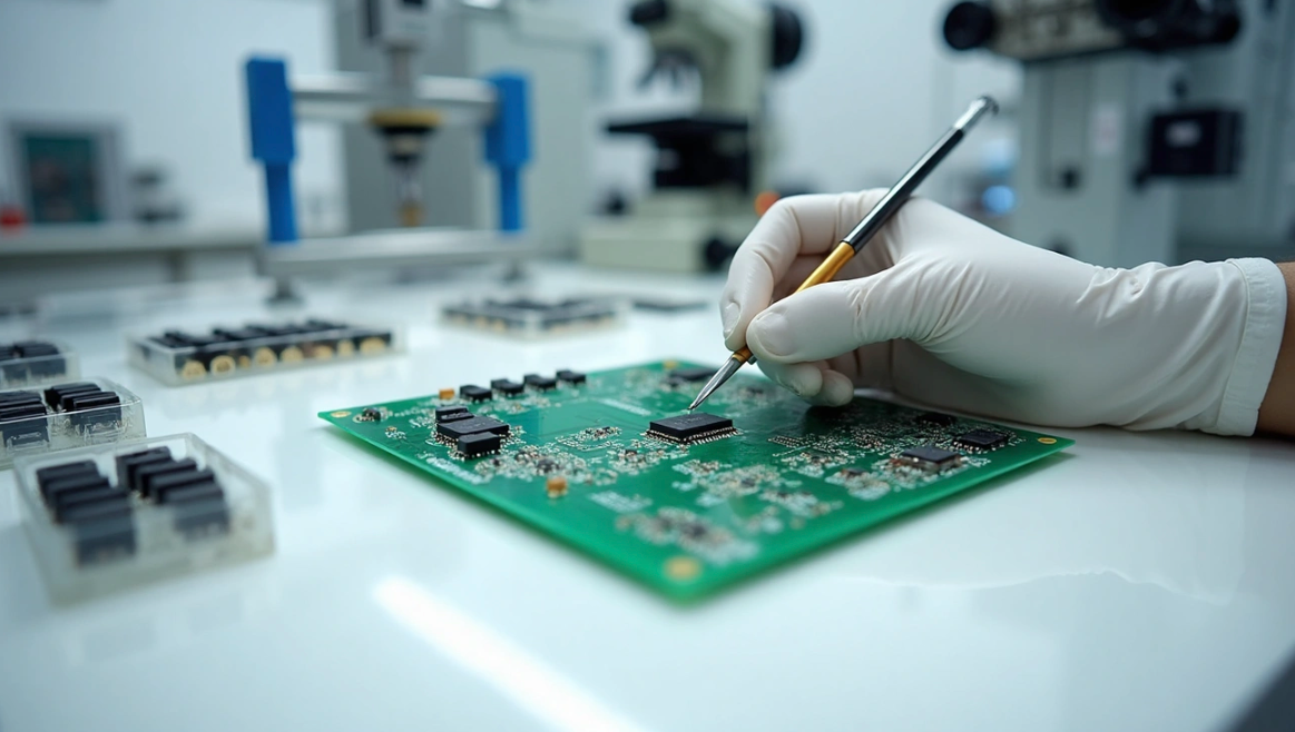
Engineers must apply solder paste with precision and perform detailed inspections before adding components to your prototype circuit board. This step stands out as maybe the most critical in PCB assembly. Such attention to detail will give a proper positioning and functionality of all joints and components. In this piece, you’ll find what each stage of the prototype PCB assembly process entails, from original design verification to final testing and production preparation.
Understanding the Role of Prototype PCB Assembly
The success of any electronic product depends on good planning and testing. This is where prototype PCB assembly makes all the difference. Mass production focuses on volume manufacturing, but prototype assembly plays a completely different role in product development.
What is PCB prototyping and why it matters
PCB prototyping turns circuit designs into real printed circuit boards that you can test and evaluate before mass production starts. Think of it as taking your design for a test drive before hitting the manufacturing highway. Engineers can confirm how things work, spot problems, and fine-tune designs with minimal risk.
PCB prototyping brings several game-changing benefits:
- Early error detection – You can spot and fix design flaws early, which stops expensive changes during later production
- Substantial cost savings – Fixing design issues gets pricier as products move closer to mass production
- Design validation—You can make sure circuits work right before investing in big manufacturing runs
- Performance optimization—you get the chance to improve functionality, reliability, and user experience through repeated testing
Prototype PCBs also work better than any drawing or simulation to show stakeholders your vision.
When to use prototype PCB assembly services
Smart timing of prototype PCB assembly saves money and time. Industry experts point to these situations where you need prototyping:
New PCB design projects – New printed circuit board designs need prototypes to check layouts, test functions, and find possible issues before large-scale manufacturing.
Design updates or revisions – Changed or upgraded PCB designs should go through prototyping to make sure the updates work as planned.
Prototype PCB assembly works best during early and middle development stages while designs evolve. Old designs that don’t need changes might not need more prototyping rounds.
Proof-of-concept validation – Engineers use prototypes to test theories that can lead to better production PCB designs.
Differences between prototype and production PCBs
Knowing what sets prototype and production PCBs apart helps set the right expectations for each development phase:
Prototype PCBs focus on keeping costs down for early concept testing. Production PCBs aim to reduce per-unit costs by scaling up manufacturing. This basic difference affects how PCBs are made.
Materials and fabrication for prototypes use easier-to-etch rolled copper and cheaper FR-4 laminates. The process aims for quick turnaround rather than perfect quality. Standard density interconnects work fine for most early tests.
Prototype PCB assembly costs more per unit but needs less upfront investment. It allows looser tolerances and needs less testing than production runs. Production PCBs need tighter tolerances, better consistency between units, and more detailed testing.
Quality prototype PCB assembly lays the groundwork for successful mass production. It proves designs work, shows manufacturing challenges, and smooths out assembly processes before scaling up.
Preparing for the Assembly Process
Your PCB design’s readiness for prototyping demands proper preparation. This preparation will give a solid foundation for assembly success. Good prep work cuts delays, lowers costs and helps your prototype match your design vision perfectly.
Required design files: Gerber, BOM, and netlist
The right design files are the foundations of successful prototype PCB assembly. You’ll need to turn your digital blueprint into formats that manufacturers understand and use:
Gerber files work as the universal language of PCB manufacturing and contain shape and location data for every element in your layout. Your PCB design’s layers need their own Gerber file to guide manufacturers on copper tracing and component placement. PCB CAD systems can create these files in RS-274X format that combines configuration parameters, apertures, XY coordinates, and commands into one file.
The Bill of Materials (BOM) is a vital part—it shows all components your prototype circuit board needs. A complete BOM has:
- Quantity of each component
- Reference designators (codes identifying individual parts)
- Component values and specifications
- Footprint information
- Manufacturer part numbers
A netlist file might seem optional but gives valuable information about electrical connections between PCB components. This file shows all “nets”—groups of pads that need electrical connections. Netlists help spot errors during PCB layout or Gerber file creation.
You’ll also need these additional files:
- Drill files showing where holes go and their sizes
- Centroid data (also called “Pick and Place” or “XY Coordinate” files) with component placement coordinates
- Assembly drawings that help when space limits stop full reference designator placement on the board
Choosing the right prototype PCB assembly manufacturer
The manufacturer you pick will substantially affect your prototype’s quality, cost, and delivery time. Here’s what to think over when looking at potential partners:
Delivery schedules should match your project timeline—some manufacturers can deliver assembled prototypes in just 5 days. The manufacturer’s past work quality and production capabilities should fit your design needs.
Great customer service and helpful resources throughout prototyping are must-haves. Partners offering full turnkey solutions make life easier by handling everything under one roof.
PCB prototyping equipment and material considerations
Materials and equipment choices shape your prototype PCB’s performance and reliability. FR-4 remains the top material choice because it insulates well and costs less, but other materials might work better for specific projects.
Modern PCB prototyping uses automated machines to make prototype boards straight from digital designs. These machines use CNC-based technologies with methods like milling, laser imaging, and inkjet printing to create detailed trace patterns.
Your prototype assembly plan should look at material needs based on:
- Operating environment conditions
- Required electrical properties
- Mechanical specifications
- Budget constraints
The actual assembly phase starts after completing these preparation steps. Components get placed and soldered according to your specifications.
Step-by-Step Breakdown of the Assembly Process
PCB prototype assembly turns your digital design into a real circuit board through several systematic steps. You should know what to expect from your prototype PCB assembly manufacturer at each stage.
Solder paste application using stencil
The assembly starts when manufacturers apply solder paste with precision. They create a stainless steel or polyimide stencil that matches your board’s surface mount pads exactly. The process needs perfect alignment – manufacturers place the stencil in an SMT device right above the PCB.
A mixture of tiny solder particles, flux, and binding agents spreads evenly across the stencil. A squeegee blade removes extra paste and lets just enough drop through onto the PCB surface. The whole process takes 15-45 seconds. Many manufacturers then run solder paste inspection (SPI) tests to check coverage quality.
Pick and place machine for component mounting
The next step puts electronic components on the board after the solder paste application. Pick and place machines do this job with amazing accuracy. These automated systems grab components from reels, trays, or feeders and put them exactly where they need to go on the PCB.
Modern equipment can place up to 47,000 components per hour in the best conditions. High-end systems achieve positioning accuracy of ±0.01mm. Even the tiniest surface mount components end up exactly where they should be before moving to the next stage.
Reflow soldering for SMT components
The PCB moves through a reflow oven on a conveyor belt once components are in place. This vital process has four temperature stages:
- Preheat: Board temperature rises 1-2°C per second to avoid thermal shock
- Soak: Temperature stays steady (150-200°C) to activate flux and heat everything evenly
- Reflow: Temperature goes above solder melting point (217-220°C for lead-free solder) to create liquid connections
- Cooling: Temperature drops 2-4°C per second so joints solidify without stress
The right temperature matters a lot – too hot damages components while too cool makes poor connections.
Manual or wave soldering for through-hole parts
Through-hole components need one of two soldering methods:
Wave soldering moves the PCB over molten solder waves. This works great for high-volume production. The process makes all through-hole component joints at once, making it quick and effective when components sit on one side.
Manual soldering needs skilled technicians to solder each joint with a soldering iron. This slower method gives better control. Prototypes, delicate components, or boards with mixed technology often need this approach to protect SMT components from wave soldering damage.
X-ray and AOI inspection for solder joint quality
Quality checks mark the final step. Automated Optical Inspection (AOI) uses high-resolution cameras to look for visible problems like missing components, solder bridges, or misalignments. AOI works fast and won’t damage anything since it never touches the board.
X-ray inspection sees through the PCB to find hidden issues that AOI misses. This helps check BGA (Ball Grid Array) components and internal connections. These inspection methods work together to ensure your prototype PCB meets quality standards before functional testing begins.
Testing and Debugging the Prototype Circuit Board
Your prototype circuit board needs extensive testing and debugging after assembly. This step determines if your design meets specifications and performs reliably under operating conditions.
Testing under ground conditions
The final electrical environment where your PCB will reside needs simulation through functional testing. Instead of looking at individual components, these tests give you a full picture of the assembly’s performance. Your prototype PCB’s behaviour under ground conditions gets verified in this last manufacturing step.
The data speaks for itself – functional testing reduces failure rates significantly. Boards with functional testing show a failure rate of 0.0003% compared to 0.03% without it. This 100-fold improvement happens because functional tests give you a full picture of circuit behaviour and verify each element’s performance.
The process includes:
- Power delivery through intended interface
- Signal application that mimics normal operation
- Output monitoring to verify correct responses
- Power issue checks including low-frequency noise and excessive jitter
In-circuit testing and signal integrity checks
In-circuit testing (ICT) confirms component placement and electrical characteristics before full board power-up. A “bed-of-nails” fixture with probes contacts test points – ICT detects 98% of manufacturing defects.
Signal integrity testing plays a vital role for high-speed channels. Simple signal integrity checks look at:
- Transmission line impedance using test fixtures with known S-parameters
- Channel losses, jitter, and distortion through direct measurements
- EMI from high-speed channels that might show impedance matching problems
- Crosstalk between parallel channels
Debugging common issues in prototype PCBs
Systematic debugging starts by finding the problem area when issues come up. Common failures include opens/shorts, excessive noise, heat problems, and unexpected logical functions.
Start troubleshooting by checking power supplies and measuring resistance between power rails and ground. A thermal inspection often shows problem areas – components that run too hot might point to short circuits or design flaws.
Voltage measurement methods help check if working voltages at key points match what you expect. Advanced tools like near-field probes and high-bandwidth oscilloscopes help identify signal integrity issues in high-speed interconnects.
A complete testing and systematic debugging process ensures your prototype PCB works correctly before production begins.
What Happens After Assembly is Complete
Your prototype’s future depends on what happens after assembly completion. Test data launches your project into a defining stage that shapes its direction.
Evaluating test results and design feedback
A structured design review must evaluate prototype PCBs thoroughly. Test engineers, manufacturers, and stakeholders provide valuable feedback. This feedback creates value only through proper documentation and tracking. Random emails or handwritten notes often miss important suggestions.
The evaluation process looks at several aspects:
- Visual inspection findings from microscopic examinations
- Voltage and current readings at test points
- Signal integrity measurements across critical traces
- Functional test results under actual operating conditions
Expert analysis spots obvious and hidden problems. These range from simple solder bridges to complex impedance mismatches that experts must interpret.
Making design revisions and re-prototyping
PCB prototyping works through iterations. The first step focuses on implementing outstanding Engineering Change Orders (ECOs) that don’t affect core functionality. Design optimisation becomes the priority next, through DFM improvements and economical solutions.
Common changes include:
- Enlarging or standardising fabrication features
- Removing unnecessary connectors, headers, or jumpers
- Resizing or removing reference designators where appropriate
- Cleaning the BOM to eliminate unsourceable components
A reliable, well-refined design usually emerges after 2-3 iteration cycles. More cycles might point to deeper design issues that need attention.
Transitioning from prototype to full production
The shift from prototype to production brings several key factors into focus. Material selection must line up with long-term product needs. Layout adjustments improve yields, and process validation ensures repeatability.
Production PCBs face stricter tolerances, regulatory inspections, and long-term reliability requirements. Small pilot runs validate the process before full production begins. Clear documentation and collaborative effort between design teams and manufacturers prove essential to success during this phase.
The Pathway Forward with Prototype PCB Assembly
Prototype PCB assembly is a vital life-blood of electronic product development. Of course, the experience from concept to working prototype needs many technical steps that require precision and expertise.
Your prototype works as planned through solder paste application, component placement, reflow soldering, and detailed inspection. Working with experienced manufacturers helps navigate these complex processes better. A good assembly partner makes your design and offers valuable feedback to improve it.
Prototype PCB assembly needs an original investment of time and resources, but it pays off through early error detection and design optimisation. On top of that, it helps speed up production scaling and cuts down development time.
Moving from prototype to production shows the peak of your development work. Your really tested design becomes ready for wider use with proven reliability and performance. This process is not just a technical need – it’s the foundation that builds successful electronic products.
Without doubt, becoming skilled at prototype PCB assembly strengthens your ability to launch innovative electronic products faster and with better quality. These basic principles help achieve soaring wins in your electronic design projects, whether you work on simple circuits or complex systems