Common Electronics Design Terms Explained: From PCB to Firmware (2025 Guide)
Understanding Common Electronics Design Terms can feel like navigating a maze, especially during complex projects. A Bill of Materials (BOM) serves as a complete list of raw materials, sub-assemblies, components, and parts needed to manufacture an end product. The document’s precision and detail play a vital role in determining production success.
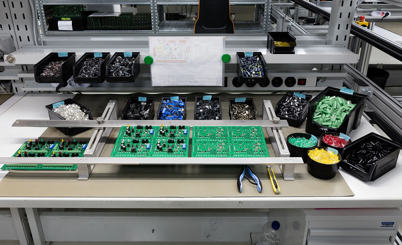
Electronics design requires a solid grasp of common components and their terminology. PCBs come to life through the combination of substrate, copper layers, solder masks, and silkscreen. Various PCB types exist – single-sided, double-sided, and multilayer boards – each designed to meet specific project needs. Quality control processes like Automated Optical Inspection (AOI) and Automated Test Equipment (ATE) ensure reliable assembled circuit boards.
This piece will help you understand the key electronics design terms you need to know in 2025. We cover everything from selecting microcontrollers based on processing needs to designing power supplies with stable voltage regulators. Your electronics design experience will become smoother as you learn about PCB layers and firmware interfaces.
Understanding PCB Layers and Their Functions
A printed circuit board (PCB) has multiple layers that create a functioning electronic device. These components stack up like a layer cake and get laminated into a single object. Each layer plays a vital role to ensure proper electrical conductivity, mechanical support, and protection of the circuit design.
Understanding PCB Layers and Their Functions
PCBs might look simple at first, but their internal structure needs careful engineering. The stackup – how conductive and insulating materials arrange – creates the foundation of your PCB. This arrangement substantially affects electromagnetic compatibility, signal integrity, and overall reliability.
Substrate and Copper Layer Roles
The substrate acts as the backbone of any PCB and provides both electrical insulation and mechanical support. We used non-conductive materials to make it, with FR-4 being the most common choice. FR-4 is a flame-retardant glass-reinforced epoxy laminate. Other options include polyimide (for flexible PCBs), metal core, and ceramic core. Engineers pick these based on what the application needs.
FR-4 remains the top choice in circuit boards of all sizes because it offers great mechanical properties, electrical characteristics, and thermal stability. Polyimide works best when you need flexibility and high-temperature resistance.
The substrate’s dielectric properties shape signal performance:
- Coefficient of Thermal Expansion (CTE): Shows how the material expands when heated, with PCB substrates typically having higher CTE than copper
- Glass Transition Temperature (Tg): The point where maximum displacement occurs on the CTE curve
- Thermal Conductivity: Most PCB substrates range between 0.3 to 0.6 W/M-ºC, much lower than copper’s 386 W/M-ºC
- Dielectric Constant: Changes signal integrity and impedance, usually dropping as frequency goes up
The copper layer sits on top of the substrate – it’s thin copper foil attached to the board with heat and adhesive. This layer creates electrical pathways that connect components. Copper thickness varies by weight, usually 1 ounce per square foot (about 35 micrometres or 1.4 thousandths of an inch). PCBs that handle high power might need 2 or 3 ounce copper.
Multi-layer boards have copper layers in pairs. Signal layers move data or power between components. Ground and power planes provide stable voltages and cut down electrical noise. You can estimate a board’s complexity by looking at its layer count and how the interconnections (vias, plated-through holes) are designed.
Solder Mask and Silkscreen Explained
The solder mask is a thin polymer coating that protects copper traces. It’s usually green but comes in other colours too. This protective layer serves several key functions:
- Stops copper traces from oxidising and corroding
- Keeps copper traces electrically isolated
- Prevents unwanted solder bridges during assembly
- Makes sure components stay in their proper spots
- Makes copper pads stronger on the board’s surface
Good solder mask design needs specific spacing rules. The distance between silk to solder mask should be at least 0.2 mm (8 mil). The solder mask web width needs to be 4 mil for green and 5 mil for other colours.
The silkscreen (or legend) is the top layer, usually in white or yellow ink. While it doesn’t affect how the circuit works, it gives important details:
- Component locations with reference designators
- Test points for measurements
- Unique board identification numbers
- Warning symbols for high voltage areas
- Polarity indicators for components
The silkscreen gets applied through Manual Screen Printing (MSP), Liquid Photo Imaging (LPI), or Direct Legend Printing (DLP). It helps during assembly, testing, and troubleshooting.
These basic PCB layers and their functions are vital knowledge for anyone in electronic design. They help you understand how common electronics components work together in the bigger system picture.
Common Electronic Components and Their Design Terms
Electronic components are the building blocks that power circuit boards. Each component has unique functions and design requirements. Anyone working with PCBs or electronic design needs to understand these elements.
Resistors, Capacitors, and Inductors
These three passive components are the foundations of almost every electronic circuit. Each one controls electrical flow differently.
Resistors limit electric current flow in a circuit and engineers measure them in ohms (Ω). They turn electrical energy into heat and help with current limiting, voltage division, and biassing in electronic circuits. You can find them in different types like carbon film and metal film. Their values range from milliohms to megaohms with tolerance values from 1% to 5%. Specialised resistors with tolerances as tight as 0.001% work well in precision applications that need exact voltage references.
Capacitors work as tiny batteries within a circuit by storing and releasing electrical energy. Two conductive plates with an insulating dielectric material between them make up their structure. Engineers measure them in farads (F), and most PCB capacitors range from picofarads (pF) to microfarads (μF). These components block DC signals but let AC signals pass through. This makes them perfect for filtering, coupling, and timing applications. They come in two types:
- Polarised (electrolytic and tantalum) that need specific directional placement
- Non-polarised (ceramic, polyester, paper) that work in any direction
Inductors create energy storage in a magnetic field during current flow. These coils of wire, often wrapped around magnetic cores, resist current flow changes. Their measurement unit is henries (H), with typical values from 1 µH to 2000 mH. Unlike capacitors, inductors block high-frequency signals while letting low-frequency signals pass.
Integrated Circuits (ICs) and Microcontrollers
ICs showcase electronic miniaturisation at its best by fitting thousands to billions of components on a single chip.
An integrated circuit combines electronic components—resistors, transistors, capacitors—into a tiny chip that works as one unit. These small “black chips” have changed modern electronics. They make devices smaller, perform better, and cost less. Compared to discrete component circuits, ICs shine in three areas: size, cost, and performance.
Engineers use two main mounting types for ICs: through-hole (PTH) and surface-mount (SMD/SMT). The Dual In-line Package (DIP) leads the through-hole category. It has two parallel pin rows spaced 0.1″ (2.54mm) apart, making it ideal for breadboarding.
Microcontrollers pack entire microcomputers into single chips that run specific programmes on repeat. Unlike regular processors, these chips focus on single automated tasks in embedded systems. A typical microcontroller has these core parts:
- CPU (Central Processing Unit) that controls all processes
- RAM (Random Access Memory) for temporary programme storage
- ROM (Read-Only Memory) holding basic instructions
- Internal Oscillator timing execution cycles
- I/O Ports connecting data signals and power
Connectors and Switches in PCB Design
Connectors and switches help electronic devices interact with users and other systems.
Connectors join active components in an assembly. PCB connectors come in several forms:
- Wire-to-board connectors linking wires to PCBs
- Board-to-board connectors joining separate PCBs
- Cable-to-board connectors connecting cables to PCBs
Most connectors use a plug and receptacle system for easy connection and separation. Today’s connector systems deliver high-density, high-speed connections. They work well with automated assembly and excel in low-voltage differential signalling applications.
Switches manage electrical current flow by creating or breaking circuit paths. They act like bridges – current flows when active and stops when inactive. PCB switches use switching circuits printed right on the board. Engineers choose from push buttons, toggle switches, rotary switches, and slide switches based on user needs and circuit requirements.
Types of PCBs and Their Use Cases
Your electronic design project’s success largely depends on choosing the right PCB type. PCB configurations come with different levels of complexity, space efficiency, and durability. These factors play a key role in your final product’s performance and cost.
Single-Sided vs Double-Sided Boards
Single-sided PCBs are the simplest PCB configuration. They have conductive traces on just one side of the substrate. These boards use a base material (usually FR-4), a thin copper layer, protective solder mask, and identifying silkscreen. This simple PCB variant gives you several benefits:
- Budget-friendly manufacturing due to fewer material needs
- Simple design and production process
- Quick troubleshooting and repair
Single-sided PCBs power many everyday devices. You’ll find them in calculators, simple LED lighting, power supplies, radio equipment, solid state drives, and simple industrial controls. But their limited routing options and lower component density make them less suitable for advanced applications.
Double-sided PCBs have conductive copper traces on both sides of the substrate. These traces connect through plated through-holes called vias. This design doubles the space for component placement and routing, which lets you:
- Create more complex circuit designs with higher component density
- Get better signal integrity and improved thermal management
- Route traces more flexibly
These features make double-sided PCBs perfect for medium-complexity applications. You’ll see them in industrial controls, HVAC systems, automotive dashboards, power supplies, amplifiers, and vending machines. Manufacturing these boards needs more steps than single-sided ones, especially when creating electrical connections between layers.
Multilayer and Flexible PCBs
Multilayer PCBs combine three or more conductive layers. These layers sandwich between insulating materials and get laminated together under heat and pressure. Modern boards can have 4 to over 50 layers, though most commercial uses need only 4-16 layers.
Multilayer PCBs give you these advantages:
- Maximum circuit density and complexity
- Better signal integrity with dedicated power and ground planes
- Enhanced thermal management and EMI shielding
These advanced PCBs power sophisticated electronic systems. Examples include computer motherboards, smartphones, telecommunications equipment, medical imaging devices, and aerospace systems. The wearable technology market values at USD 219.3 billion in 2025. Experts predict it will reach USD 493.26 billion by 2030, growing at 17.6% yearly.
Flexible PCBs bring something different to circuit design. They use thin, bendable materials like polyimide or polyester. These materials let the conductive traces bend and twist without damage. You can get them in single, double, or multilayer versions. Flexible PCBs stand out because they:
- Can fit into 3D spaces by conforming to irregular shapes
- Last through 10,000-100,000+ bending cycles
- Weigh 60-80% less than similar rigid boards
These features make flexible PCBs great for special applications. They work well in mobile phone displays, wearable technology, medical sensors, and aerospace systems where parts must fit irregular shapes or resist vibration.
Rigid-Flex PCBs in Wearables
Rigid-flex PCBs blend rigid sections for mounting components with flexible connections in one piece. This smart design removes the need for connectors between board parts, which:
- Makes the board more reliable by reducing failure points
- Lets you package components in 3D spaces
- Keeps signals strong across all board sections
Rigid-flex PCBs have become crucial in today’s growing wearables market. They work like the nervous system in smartwatches, fitness trackers, and medical wearables. Designers can now create products that are compact, comfortable, and tough.
A smartwatch shows how useful rigid-flex PCBs can be. The board wraps around corners and fits in tight spaces without extra wires. Main chips sit securely on rigid sections while flexible parts connect the screen, battery, and sensors. Health monitoring patches that stick to skin also benefit from this design. The boards flex as people move.
Fitness trackers need rigid-flex PCBs too. These boards connect many sensors and batteries inside small cases. This technology now forms the backbone of modern wearable electronics. It supports both style and function in increasingly advanced devices.
Key Design Terms in PCB Layout
A PCB’s physical layout does more than connect components – it directly impacts signal integrity, power delivery, and reliability. Engineers who grasp these basic design terms can build efficient and functional electronic circuits.
Traces, Pads, and Vias
Traces work like roads on a PCB. These thin copper lines create conductive paths that carry electrical signals between components. The width of these copper pathways plays a vital role – wider traces handle more current, while thinner ones help save board space. Most low-current analogue and digital signals work well with a 10-mil trace width.
Pads are landing zones where component leads connect through soldering. These small metal areas bind components both mechanically and electrically to the board. You’ll find two main types: through-hole pads with holes for component leads, and surface-mount pads that provide flat areas for smaller components. The pad’s soldering ring needs at least 0.20 mm width to give reliable adhesion and electrical connectivity.
Vias create tunnels between PCB layers so signals can move through multi-layer boards. These plated holes connect traces across different layers. Three main types exist:
- Through-hole vias that run through the entire board
- Blind vias that link outer layers to inner ones
- Buried vias that connect only inner layers
Standard plated through-hole (PTH) diameter measures about 8 mil (0.2 mm), while buried via holes (BVH) run around 4 mil (0.1 mm). The via’s soldering ring should be at least 0.15 mm wide for reliability.
Ground Plane and Power Plane Definitions
A ground plane is a large copper area that gives signals a common reference point and creates current return paths. This conductive layer helps reduce noise and electromagnetic interference (EMI) by offering a low-impedance path for return currents, which helps maintain signal integrity.
Power planes are copper layers dedicated to distributing power supply voltages across the board. These planes deliver steady voltage throughout the PCB and help prevent voltage drops. Working with ground planes, they help deliver consistent power and stop brown-out issues when power needs spike suddenly.
Both planes make circuit design easier by removing the need to route individual power and ground traces manually. The best results come from extending power planes across the entire PCB to create low impedance paths. Designers should watch return current paths carefully to avoid signal problems, especially in mixed-signal designs.
Clearance and Impedance Control
Clearance measures the space between conductive elements on a PCB. This spacing stops short circuits and keeps electrical components isolated. Good clearance design prevents electrical arcing and keeps circuits running reliably. CAD tools check if designs meet clearance rules as a key step in PCB design.
Impedance control becomes critical in high-speed PCB designs, especially for signals above 100 MHz. It keeps electrical impedance consistent along signal traces to prevent distortion, reflections, and data loss. USB 2.0 signals need 90 ohms of differential impedance – even a 10% change can degrade signals substantially.
Many factors affect impedance: trace width, trace thickness, dielectric material properties, and the space between traces and reference planes. Standard 1.6mm FR-4 boards often use 0.3mm trace width with 0.2mm dielectric height for single-ended 50-ohm traces. Differential pairs aiming for 90 ohms typically use equal trace widths (about 0.2mm) spaced around 0.3mm apart.
Becoming skilled at these PCB layout terms will help you create reliable, high-performance electronic designs.
Manufacturing and Assembly Terminology
Electronic device production depends on specialised manufacturing and assembly techniques that connect design to final product. These processes determine how durable, reliable, and affordable electronic assemblies will be.
Surface Mount Technology (SMT)
SMT brought a new way to assemble PCBs by mounting components directly on the board’s surface instead of through holes. Surface Mount Devices (SMDs) come with small leads or no leads, which allows them to be soldered right onto conductive pads. The SMT assembly works through several key steps.
The process starts with applying solder paste (a sticky mix of flux and tiny solder particles) to the board’s pads using a stencil. Automated pick-and-place machines then position components with precision. The assembly moves through a reflow oven where solder melts and creates secure connections.
This technology brings remarkable benefits. We mounted components on both sides of the PCB, which allows for higher density. SMT now replaces older methods in many cases because it creates smaller boards, reduces product weight, simplifies fabrication, and speeds up circuitry.
Through-Hole Technology (THT)
THT, also known as “thru-hole,” mounts components by inserting leads through pre-drilled PCB holes and soldering them on the opposite side. This classic method creates strong mechanical connections that work perfectly for applications needing high reliability.
THT assembly needs holes drilled based on component requirements. Component leads go through these holes and get soldered onto pads on the bottom side. While it takes more space than SMT, THT delivers better durability – perfect for components that face mechanical stress, high temperatures, or vibration.
Many applications still need THT, including power electronics, military and aerospace systems, industrial automation, medical equipment, and automotive systems.
Reflow and Wave Soldering Methods
Reflow soldering works best with SMT assembly. This method melts pre-applied solder paste in a controlled-temperature oven to create lasting joints. Temperature follows a specific pattern: preheat, thermal soak, reflow (melting solder), and cooling.
Wave soldering takes a different approach. PCBs pass over a wave of molten solder that creates connections quickly. This method suits THT components best and involves flux application, board preheating, solder wave exposure, and cooling. Wave soldering moves faster than reflow, making it ideal for high-volume production.
Manufacturers often use both methods on the same board for mixed-technology assemblies. When boards have SMT and THT components, they first use reflow soldering for surface mount parts and then wave soldering for through-hole components.
Testing and Quality Control Terms
Quality assurance is a vital phase in electronics manufacturing that uses rigorous testing methods to verify product functionality and reliability. Electronics continue to grow more complex. Multiple testing approaches work together to identify potential risks before products reach consumers.
In-Circuit Testing (ICT)
In-Circuit Testing gets into individual components and connections on a PCB to detect manufacturing defects. This white-box testing method verifies shorts, opens, resistance, capacitance, and other simple quantities to confirm proper fabrication. A “bed-of-nails” test fixture serves as the typical ICT equipment—an array of spring-loaded pins makes contact with specific test points on the circuit board.
ICT offers these key advantages:
- Component-level fault diagnosis
- Reduced production downtime by identifying defects early
- Quick detection of manufacturing errors including short circuits and incorrect component values
ICT has limitations because it cannot test parallel components effectively and needs test access points designed into the PCB. Manufacturers often combine ICT with other methods to achieve detailed testing.
Functional Testing and Continuity Checks
Functional Testing assesses the overall functionality of a finished electronic product through real-life usage scenarios, while ICT gets into individual components. This testing verifies that assembled products meet quality and performance standards before shipping to customers. It identifies defects not detectable through ICT such as software issues or mechanical failures.
Teams perform functional testing after prototype fabrication and test the system against predetermined performance requirements. Individual components undergo testing only if the board fails, then the root cause needs isolation to a specific component.
Continuity testing is a simple diagnostic method that checks if an electrical path exists between two points in a circuit. A complete path shows a closed circuit with proper connections. Most digital multimeters come with a dedicated continuity mode. The metre beeps when it detects a complete path, so technicians can focus on testing without watching the display constantly.
AOI and X-ray Inspection
Complex assemblies need visual inspection methods to provide significant verification. Automated Optical Inspection (AOI) automatically inspects PCB components and solder joint quality with cameras and image processing algorithms. AOI systems detect surface-level defects like missing components, misalignment, and visible solder problems.
X-ray Inspection reveals hidden defects that optical systems cannot see. This non-destructive method uses X-rays to get into internal structures, which works especially well to inspect Ball Grid Arrays (BGAs) or hidden solder joints. The technology creates detailed images by detecting variations in material density. Heavier elements like solder absorb more X-rays than lighter materials such as plastic or fibreglass.
Manufacturers often implement multiple testing methodologies throughout the production process in applications where reliability matters most. This creates a detailed quality control system that will give a guarantee that electronic products perform as designed.
Firmware-Related Design Terms
Firmware acts as an invisible bridge between hardware and software in electronic systems. It controls low-level hardware functions through specialised code stored in non-volatile memory. Electronic designers and troubleshooters must know these firmware-related terms to work effectively.
Bootloader and Flash Memory
The bootloader is the first code that runs when a device starts up. It initialises hardware components and prepares the environment for the main firmware. This vital programme lets you update firmware without specialised hardware programmers. Bootloaders stay in flash memory or ROM and keep working even when devices turn off. Many microcontrollers store bootloaders in dedicated flash memory areas to stop accidental corruption or unauthorised changes.
Flash memory holds the firmware and lets you reprogram it – a process known as “flashing.” You can update existing firmware with new data to upgrade devices without replacing hardware. Flash memory works great in devices that need to save space.
SWD and JTAG Interfaces
Serial Wire Debug (SWD) is a simple debugging protocol made for ARM processors. It needs just two main pins—SWDIO (data) and SWCLK (clock). This setup helps you programme and debug while using minimal board space. SWD shines when PCB layout has limits or pin resources are tight.
JTAG (Joint Test Action Group) provides more debugging options and was created to test integrated circuits. It uses several pins including TCK (Test Clock), TDI (Test Data In), TDO (Test Data Out), and TMS (Test Mode Select). Developers can set breakpoints and walk through code on actual devices with both interfaces.
Real-Time Operating System (RTOS)
A Real-Time Operating System handles task scheduling for time-sensitive embedded applications. It makes sure critical operations happen when they should. Unlike regular operating systems, an RTOS delivers predictable behaviour through priority-based preemptive scheduling—running the most important task that’s ready.
RTOSes come in three types based on timing needs:
- Hard real-time systems—missing deadlines causes serious problems
- Firm real-time systems—can handle some delays without major issues
- Soft real-time systems—timing matters but missed deadlines aren’t critical
These specialised systems make complex applications easier by managing timing requirements. Developers can focus on core functionality instead of timing details.
Common Acronyms in Electronics Design (2025 Update)
Common Acronyms in Electronics Design (2025 Update)
Electronics designers use a specialised language of acronyms to communicate efficiently. These shortcuts are crucial if you work with circuit designs or documentation.
BOM, DFM, DRC, and ESD
BOM (Bill of Materials) has a detailed list of all components, raw materials, and subassemblies needed to make an end product. DFM (Design For Manufacturing) helps create products that are easier to fabricate, yield better results, and cost less to produce. DRC (Design Rule Check) makes sure PCB layouts meet manufacturing capabilities and constraints. ESD (Electrostatic Discharge) happens when electricity suddenly flows between objects with different electrostatic potentials, which can damage sensitive components.
SMT, PCB, IC, and MCU
SMT (Surface Mount Technology) lets you attach electrical components directly to a board’s surface instead of through plated holes. PCB (Printed Circuit Board) serves as the base where electronic components sit. IC (Integrated Circuit) has a complete circuit made on a silicon chip, mounted in a package. MCU (Microcontroller Unit) works as a compact integrated circuit that controls specific operations in embedded systems.
CAD, CAM, and Gerber Files
CAD (Computer Aided Design) makes shared design creation and product visualisation possible on graphics screens. CAM (Computer Aided Manufacturing) uses computer systems throughout manufacturing phases. Gerber Files serve as universal blueprints between designers and manufacturers, containing all PCB layer information.
Conclusion
This piece explores the complex world of electronics design terminology. Understanding these terms is the life-blood of working with electronic systems. Each element plays a vital role in successful electronics design, from basic PCB layers like substrates and copper traces to specialised components that bring circuits to life.
PCBs come in many forms – from simple single-sided boards to complex multilayer and flexible configurations that offer solutions for specific applications. Rigid-flex PCBs have revolutionised wearable technology and let designers create compact yet functional devices.
Design terms like traces, pads, vias, and impedance control might look technical at first. But becoming skilled at these concepts helps create reliable circuits. Manufacturing processes like SMT and THT connect design with physical products. Testing methods make sure devices work properly before reaching end-users.
Firmware terms create the vital link between hardware and software, though people often overlook them. Bootloaders, flash memory, debugging interfaces, and RTOSes work quietly to enable the continuous operation we expect from modern devices.
The acronyms section helps decode electronics design’s specialised language. These shorthand terms make it easier to communicate with professionals and direct newcomers through technical documentation.
Electronics keeps evolving. Staying up to date with these terms will help you design better and communicate clearly with colleagues and manufacturers. You can use this piece as your reference point when you find unfamiliar terminology during your design work. This approach will make your projects run smoothly and successfully.
FAQs
Q1. What are the main types of PCB testing methods? There are several key PCB testing methods, including visual inspection, in-circuit testing (ICT), flying probe testing (FPT), automated optical inspection (AOI), X-ray inspection, burn-in testing, and functional testing (FCT). Each method serves a specific purpose in ensuring the quality and functionality of printed circuit boards.
Q2. What is a fundamental rule for PCB design? A basic rule in PCB design is to maintain proper clearances. Components and connectors should be at least 0.04″ (40 mils) away from the board edge, while drill holes and copper traces should be at least 0.010″ (10 mils) from the edge. It’s also crucial to ensure that footprint pads match the components listed in the Bill of Materials (BOM).
Q3. Which PCB design software is widely used in the industry? Several popular PCB design software options are available, including PADS by Siemens, Autodesk Eagle, DipTrace, KiCad EDA, and DesignSpark PCB. These tools offer various features for schematic capture, PCB layout, and design validation, catering to different user needs and project complexities.
Q4. What is the purpose of vias in PCB design? Vias are small drilled holes that connect two or more adjacent layers in a PCB. They allow signals and power to travel between layers, establishing inter-layer connections. Vias are crucial in multilayer PCBs where circuits between layers are independent, enabling complex routing and improved board functionality.
Q5. What are the advantages of Surface Mount Technology (SMT) in PCB assembly? Surface Mount Technology (SMT) offers several benefits in PCB assembly. It allows for higher component density as parts can be mounted on both sides of the board. SMT also enables smaller board sizes, reduced product weight, simplified fabrication processes, and faster circuitry. These advantages have made SMT the preferred method for many modern electronic applications.